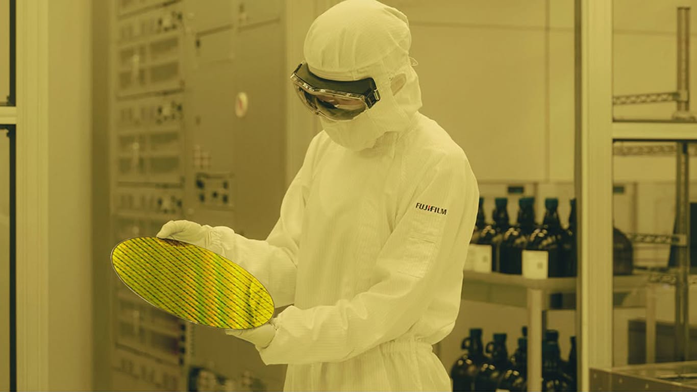
FUJIFILM Corporation will expand its semiconductor materials business by enhancing production facilities for copper interconnect CMP (Chemical Mechanical Planarization) slurries at the FUJIFILM Electronic Materials U.S.A., Inc. production site in Mesa, Arizona. Fujifilm will also establish new production facilities capable of multi-product manufacturing of CMP slurries for diversified semiconductor manufacturing processes, including advanced packaging applications.
The investment, totaling $18 million, addresses increasing demand for copper interconnect CMP slurries, and supports long-term growth in advanced logic, advanced memory and advanced packaging applications.
DEEPER DIVE: Mesa approves $3 billion Legacy Park development
“The advanced semiconductor market has entered a period of significant growth, driven by the rapid expansion of demand related to artificial intelligence,” says Brian O’Donnelly, president and CEO, FUJIFILM Electronic Materials U.S.A., Inc. and corporate vice president, FUJIFILM Corporation. “As global semiconductor demand continues to increase, demand for CMP slurries—an essential material used in advanced semiconductor manufacturing—is also growing.”
In particular, demand for CMP slurry for copper interconnects, a product for which Fujifilm has a leading global market share, is increasing in the advanced logic and memory sectors.
In the United States, major semiconductor manufacturers continue to invest in new and expanded production facilities, resulting in high demand for semiconductor materials. In response to these market conditions, FUJIFILM Electronic Materials U.S.A., Inc will expand its CMP slurry production in Mesa, Arizona. In addition to expanding capacity for copper interconnect CMP slurries used in BEOL processes, Fujifilm will establish new production facilities capable of manufacturing a wide range of CMP slurry products for FEOL, MOL and advanced packaging applications, including hybrid bonding. The new production facilities will serve as a bridge between product development and commercial manufacturing, enabling technologies developed at the Arizona site’s global CMP slurry R&D center to be transferred quickly into mass production.
The expanded production line is scheduled to begin operations in 2027. Once operational, CMP slurry production capacity at Fujifilm’s Mesa facility will further support medium- and long-term growth in demand.
Going forward, Fujifilm will continue to provide a broad portfolio covering nearly all semiconductor manufacturing processes, from leading-edge to legacy nodes.
Leveraging its global manufacturing network across Japan, the United States, Europe and Asia, together with its strong R&D capabilities, Fujifilm will offer one-stop solutions that help address customers’ challenges and contribute to the continued development of the semiconductor industry.