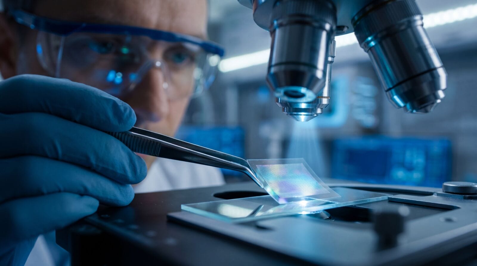
From smartphones and electric vehicles to medical devices and artificial intelligence, nearly every aspect of modern life depends on semiconductors. But after decades of making computer chips smaller and more powerful, the industry is reaching practical limits.
The next leap forward may come from a different approach known as advanced packaging — combining multiple specialized little chips, or “chiplets,” into a single package that delivers greater performance while using less space and energy.
Work at Arizona State University’s MacroTechnology Works is advancing that future.
Jason Conrad, chief operating officer of ASU’s Southwest Advanced Prototyping, or SWAP, Hub and site lead for MacroTechnology Works, recently discussed how ASU is helping industry develop next-generation semiconductor technologies while preparing the workforce that will build them.
DEEPER DIVE: TSMC Arizona’s thoughtful plan for managing water use
LEARN MORE: TSMC Arizona preparing workers for a chips future
Note: The following questions and answers have been edited and condensed for clarity from an interview Conrad shared with Dan Marrujo, host of the “Micro Journeys” podcast. Watch the complete conversation during this podcast episode.
Question: Why is the semiconductors sector getting so much attention right now?
Answer: Semiconductors power almost everything we use today, and as that technology becomes more important, so does the ability to design, manufacture and improve it here in the United States.
Arizona is seeing tremendous investment from the semiconductor industry, and ASU is right at the center of that ecosystem. At our MacroTechnology Works, we’re investing in new capabilities, partnering with companies large and small, and helping develop both new technologies and the workforce needed to support them. It’s an exciting time because we’re bringing together higher education, industry and government to accelerate innovation and help move ideas into real-world applications.
Q: What is “advanced packaging,” and why is it such a big deal?
A: Traditionally, a computer chip is packaged inside a protective case that connects it to the rest of an electronic system. For many years, most of the industry’s effort focused on making a single piece of silicon more powerful by shrinking the transistors on it.
But we’re reaching the practical and economic limits of that approach. Instead of asking one chip to do everything, advanced packaging lets us separate different functions — such as memory, logic and power — into separate chiplets and combine them into a single package.
That approach offers advantages in size, weight, power consumption and cost. It also gives designers much more flexibility because they can combine different kinds of technologies in ways that weren’t possible before.
Q: What makes ASU’s MacroTechnology Works different from a typical university research facility?
A: Everything we do is driven by connections with industry. MacroTechnology Works is a former semiconductor fabrication site, and we’re co-located with companies ranging from startups to major technology firms.
We’re also conducting research and development using the same types of equipment found in leading semiconductor manufacturing facilities. And because we’re working with industry-standard tools, we can help accelerate the transition from research to commercial production.
Our mission is really to bridge what people call the “valley of death” between discoveries made in the laboratory and products that are manufactured at scale and make an impact in the world.
Q: How are ASU students benefiting from this work?
A: Universities are known for educating students, and that’s still our mission. But we’re doing it in a different way.
Students are working alongside industry on current, real-world engineering challenges using the same equipment and technologies they’ll encounter after graduation. This means they leave ASU with hands-on experience that is directly relevant to the workforce.
One area where that’s especially important is advanced packaging. For years, the United States didn’t have much of a domestic packaging industry, so students had very little opportunity to learn those skills. We’re changing that by giving students the chance not only to study advanced packaging but to see it and do it at our MacroTechnology Works.
Q: Why has Arizona become such an important place for semiconductor innovation?
A: Arizona has built an extraordinary semiconductor ecosystem over many decades. Major manufacturers, suppliers, startups and research organizations are all investing here, and ASU plays an important role in connecting these elements.
Our investments at MacroTechnology Works, together with our partnerships across industry, create infrastructure that companies can use to develop new technologies more quickly. We also help prepare the workforce those companies need as they continue to grow.
It’s really the combination of education, research and industry that makes Arizona such a strong place for innovation.
Q: How does ASU help companies turn ideas into real products?
A: We work with companies at many different stages — from established industry leaders to early-stage startups.
Sometimes they’re looking for access to specialized equipment. Sometimes they’re seeking technical expertise or research partners. Sometimes they simply have a promising idea and need help figuring out how to develop it.
Our goal is to connect people with the capabilities and expertise they need so they can move from just an idea to a working prototype and, ultimately, to manufacturing. By opening access to these facilities and bringing together researchers, students and industry partners, we help accelerate innovation.
Q: What do you hope the SWAP Hub will accomplish over the next several years?
A: We’re now focusing on execution — making these capabilities available to our partners and building a sustainable ecosystem for the future.
Success means continuing to work with industry and government partners, winning new research opportunities, refreshing our facilities with state-of-the-art equipment and expanding workforce development programs.
Ultimately, our mission is to help move technology from the laboratory into manufacturing, where it can make a real difference. When you bring together companies, students and faculty around meaningful challenges, you create an environment where innovation can thrive.
Learn more about how ASU is powering the future of America’s semiconductor sector and more at microelectronics.asu.edu.