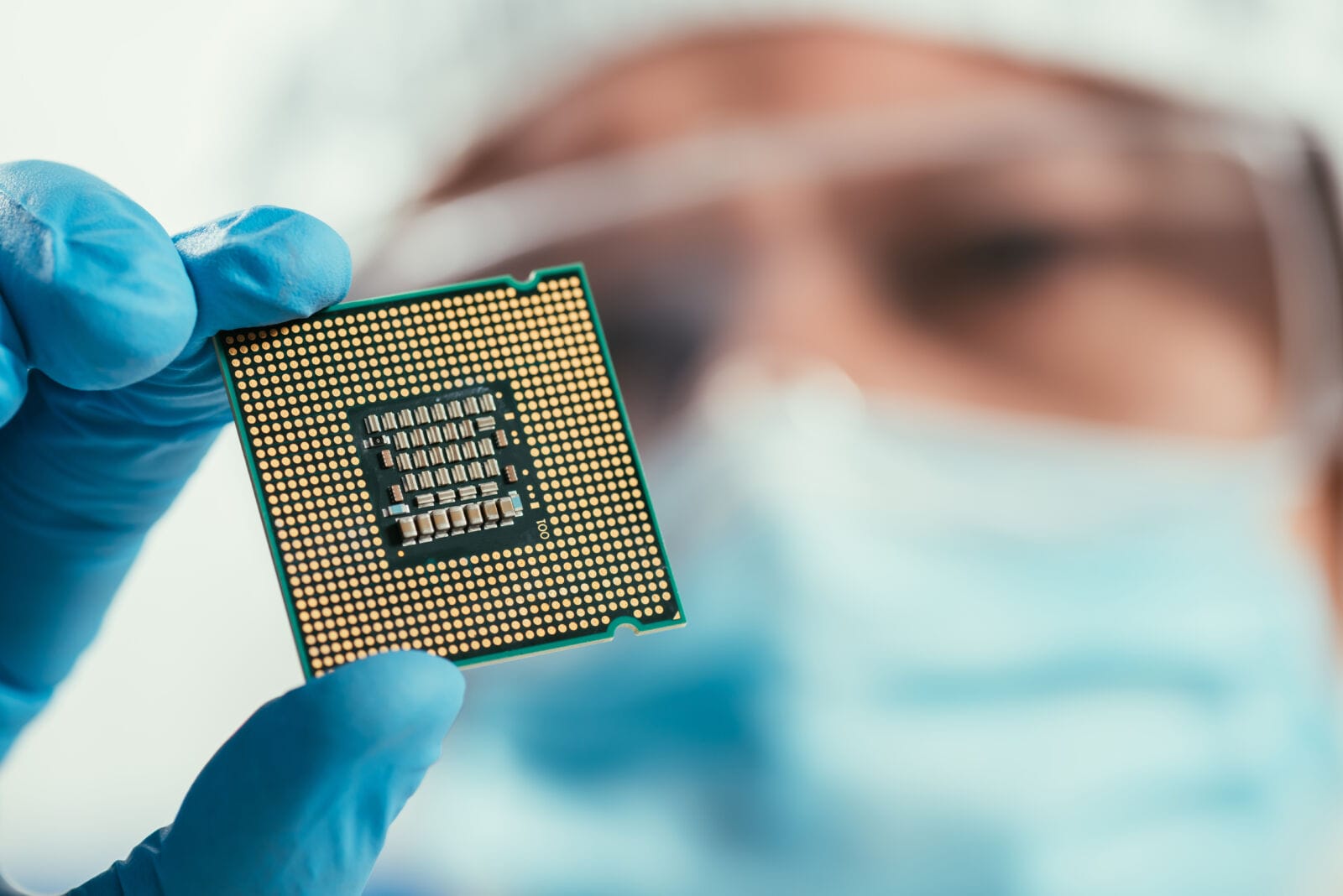
Semiconductor performance often gets most of the attention, but a chip cannot function alone. After fabrication, the die must be connected, supported, protected, and integrated into a larger electronic system. This makes packaging an important part of semiconductor manufacturing. For selected thin metal components used around packaging and electronics, chemical etching provides a flexible way to create fine, repeated, and complex flat geometries.
As packages become smaller and connection density increases, the physical components around the semiconductor must also become more precise.
What Is Semiconductor Packaging?
Semiconductor packaging protects the die and creates the connection between the chip and the outside circuit.
A simplified packaging structure may include:
- Semiconductor die.
- Die pad or support structure.
- Electrical leads.
- Bond wires or other interconnects.
- Protective package material.
- External contacts.
The exact design varies by package type.
Some modern packages use advanced substrates, redistribution layers, or chiplet architectures. Others still depend on metal lead frames as part of the mechanical and electrical structure.
The important point is that packaging is not only about protecting silicon. It also creates the physical path between the die and the final electronic system.
Why Precision Matters in Semiconductor Packaging
Semiconductor packages continue to become smaller while supporting more connections and higher device density.
This creates several manufacturing challenges.
Smaller Features
Lead fingers, slots, openings, and connection areas may need to fit within a limited package footprint.
Repeated Geometry
A production strip can contain many identical lead-frame units. Consistency across the pattern matters for later assembly and forming.
Thin Materials
Packaging components often use thin metal to reduce size and support compact structures.
Alignment
The die, leads, bonding areas, and package geometry must work together during assembly.
These requirements make the manufacturing method an important part of package design.
The Role of Lead Frames
A lead frame is a thin metal structure used in many semiconductor and electronic packages.
It can provide mechanical support for the die while creating electrical paths between the semiconductor and external circuitry.
A typical lead frame may include:
- Die pad.
- Lead fingers.
- Tie bars.
- Outer frame.
- Indexing features.
- Repeated package patterns.
Precision lead frames can be produced from metals such as copper alloys and other suitable thin sheet materials, depending on the electrical, mechanical, and packaging requirements.
The final component may also require plating, forming, cleaning, or other secondary operations.
How Chemical Etching Produces Lead Frames
Chemical etching, also called photochemical etching or photochemical machining, removes selected areas from a metal sheet.
The process begins by cleaning the metal and applying a light-sensitive photoresist.
Digital artwork defines the lead-frame geometry. Ultraviolet exposure transfers that pattern to the coated sheet.
After development, an etchant removes the unprotected metal.
The finished sheet can contain fine leads, slots, openings, die-pad features, indexing details, and complex outer profiles.
Because the pattern is created from digital artwork, several detailed features can be produced within the same flat design.
Why Chemical Etching Fits Precision Packaging Components
Chemical etching offers several advantages for selected thin packaging components.
Fine Flat Geometry
Lead frames can contain many narrow features and repeated patterns.
Photochemical processing defines these features through the same artwork rather than machining them individually.
No Direct Mechanical Cutting Force
Stamping uses mechanical force to cut sheet metal.
Chemical etching removes material through a controlled chemical reaction, so no cutting tool presses directly against the thin sheet during profile creation.
This can be useful for delicate or detailed geometries.
No Laser Heat-Affected Zone
Laser cutting uses concentrated heat to remove material.
Chemical etching does not use a laser beam to form the profile, so it avoids laser-related heat-affected zones.
Digital Design Changes
Semiconductor package development can require several design revisions.
Engineers may change:
- Lead geometry.
- Lead spacing.
- Die-pad dimensions.
- Outer frame design.
- Alignment features.
With chemical etching, many of these changes can be made by updating the digital phototool rather than building a new hard cutting die for every revision.
Chemical Etching vs Stamping
Chemical etching and stamping can both be used for thin metal components, but they serve different manufacturing situations.
Chemical etching is often attractive during prototype development, engineering validation, and programs involving complex flat geometry or multiple design versions.
The lower dependence on dedicated hard tooling makes design changes easier to evaluate.
Stamping becomes more attractive when the component design is stable and production volume is very high.
Once a production die is developed and validated, stamping can achieve strong unit economics for repeated parts.
This means the correct question is not whether etching or stamping is universally better.
The better question is whether the design is stable, how complex the geometry is, and what production volume is expected.
From Prototype to Production
Semiconductor packaging development usually moves through several stages.
A simplified path may look like:
Design → Prototype → Engineering Validation → Pilot Build → Production
During early development, teams may need to adjust package size, lead geometry, spacing, or assembly features.
Flexible tooling helps engineers make these changes before committing to mature high-volume production.
Chemical etching can support prototype and selected repeat-production programs when the component geometry remains suitable for the process.
As volume increases, manufacturers can also compare the cost and capability of etching with stamping or other production methods.
Precision Metal Components Beyond Lead Frames
Semiconductor and electronic assemblies may also use other thin metal parts.
Precision metal shims can help control spacing, alignment, or assembly height around electronic modules and mechanical structures.
Other chemically etched components may include:
- Electrical contacts.
- Fine metal screens.
- Sensor apertures.
- Flat springs.
- Shielding blanks.
- Thin support plates.
Each part should be evaluated according to its material, thickness, geometry, tolerance, production volume, and secondary-processing requirements.
Chemical Etching Is Not a Semiconductor Wafer Process
It is important to separate two different uses of the word “etching.”
Semiconductor fabrication uses highly specialized wet and dry etching processes to create microscopic structures on wafers.
Photochemical metal etching, by contrast, is used to manufacture precision components from metal sheet.
The processes operate at different stages of the semiconductor supply chain.
For packaging applications, chemical etching is relevant to selected metal components such as lead frames and related thin precision parts, not to the fabrication of transistor structures inside the silicon die.
Precision Packaging Supports the Complete Device
The semiconductor industry depends on more than advanced wafer fabrication.
A finished chip must also be packaged, connected, protected, tested, and integrated into an electronic system.
Lead frames and other precision metal parts represent one physical layer within that process.
For thin components with fine, repeated, and complex flat geometries, chemical etching can provide a flexible manufacturing route that supports design changes without requiring a dedicated hard cutting die for every revision.
As semiconductor packages continue to become smaller and more integrated, selecting the right manufacturing process for these precision components will remain an important part of packaging design.