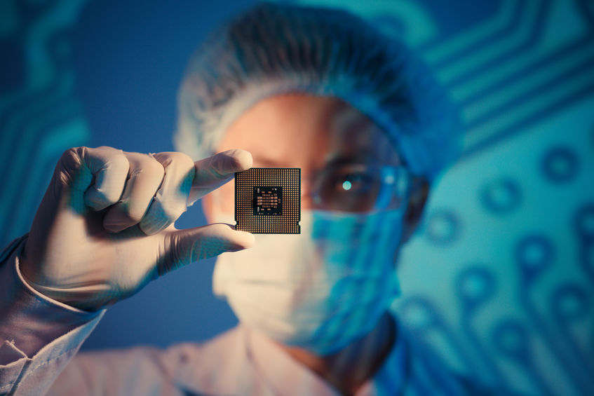
Silicon is an example of a semiconductor, materials that have the characteristics of both a conductor, such as copper, and an insulator, like glass, allowing engineers to precisely dial in exact electricity flow under specific conditions. This makes semiconductors well-suited for building the microscopic circuits at the heart of the computers in our devices.
Every year, more than a trillion semiconductors roll off assembly lines to meet an insatiable appetite for microelectronics that are faster, smarter, cheaper; demand is growing.
The U.S., birthplace of semiconductors, was once the global manufacturing leader. But over the past few decades, competition drove many manufacturers abroad. According to the Semiconductor Industry Association, today the U.S. manufactures about 12% of the world’s semiconductors.
READ ALSO: Intel’s $20 billion Arizona expansion will bring 3,000 new high-wage jobs
READ ALSO: Taiwan Semiconductor launches $38B Phoenix presence by signing major lease
The coronavirus pandemic exposed the risks of relying on an international supply chain for a critical product. As the virus circled the globe, worldwide semiconductor manufacturing facilities — called fabs — came to a standstill. Suddenly, no one could get their hands on the chips that power the modern world. The shortage has held up production for cars, televisions, washing machines and even smart toasters.
Politicians in Washington, D.C., realized that semiconductor manufacturing in the U.S. is a matter of national security. When President Joe Biden announced his administration’s $2 trillion infrastructure bill, he held a semiconductor chip aloft to underscore the industry’s prominent place in the bill.
“This is infrastructure,” Biden said. “We’ve been falling behind on research and development and manufacturing, and, to put it bluntly, we have to step up our game.”
Sally C. Morton, executive vice president of Arizona State University’s Knowledge Enterprise, agrees. She highlights the fundamental importance of semiconductor chips in our daily lives and in national security.
“Everyone is impacted by semiconductors, but we don’t always see all the ways that microchips support the lives we lead,” Morton says. “We need to have autonomy in this space for both production and distribution.”
![]()
Arizona’s chip investment
Because of strong historical roots and rapid expansion, Arizona is poised to be at the epicenter of the American semiconductor revolution, with ASU playing a starring role. Last spring, two of the world’s largest chipmakers, Intel and Taiwan Semiconductor Manufacturing Company, announced plans to spend a combined $32 billion building three semiconductor fabs in the Phoenix region, with TSMC purchasing enough land to possibly build five more fabs, which would invest billions of dollars more. Around the same time, Samsung shortlisted Phoenix as a possible factory site.
The interest in Phoenix makes sense. For decades, city officials, business leaders and ASU cultivated the infrastructure, regulatory environment and human talent the industry needs. And their timing couldn’t have been better. Worldwide semiconductor industry sales hit $439 billion in 2020, according to the SIA, with the industry projected to reach $803.15 billion by 2028.
“Building up the semiconductor ecosystem in this state will bring industry and jobs,” Morton says. “This is an economic opportunity that improves our well-being.”
Local partnerships, global impact
When Michael Kozicki, a professor of electrical engineering and director of the Center for Applied Nanoionics, first arrived at ASU in 1985, semiconductor manufacturing had already established a foothold in the area. Intel and Motorola anchored it, building a foundation that includes NXP, ON Semiconductor, Microchip Technology, Medtronic and others.
Kozicki’s ability to straddle the divide between industry and academia has proved invaluable for preparing generations of Sun Devils for careers at the world’s largest chipmakers. Today, he leads courses covering everything from working in the planet’s cleanest laboratories to designing next-gen chips, a heady mixture of practical and experimental knowledge that students need to drive nonstop innovation in microelectronic engineering.
“There are not many universities that do courses in semiconductor fabrication where you get a hands-on, industry-relevant education,” Kozicki says. “It’s all part of getting people ready to be productive professionals within the semiconductor industry. We’re a major supplier of talent.”
ASU’s emphasis on industry-relevant research has forged mutually beneficial partnerships with local semiconductor firms. In 2017, for example, the university partnered with ON Semiconductor, a Phoenix-based supplier to the global industry, to establish a $2 million, five-year award to support two ASU professors working on the leading engineering and supply chain issues faced by manufacturers.
One of the award recipients is Bertan Bakkaloglu, a professor of electrical engineering. His research focuses on analog circuit design. It’s foundational for the emerging Internet of Things, connecting machines to the web to monitor and control them remotely. To turn off lightbulbs while away, a conventional copper switch isn’t going to cut it.
Bakkaloglu says the ON Semiconductor professorship critically supports his students’ research efforts. Manufacturing small batches of experimental semiconductor chips can cost tens of thousands of dollars. Still, the process of taking a chip from concept to fabrication is a critical experience that prepares students for the industry’s challenges.

“Our students gain experience in areas that almost every semiconductor company in town requires,” Bakkaloglu says. “My PhDs don’t go to the Bay Area or Texas. They stay in Arizona. So it’s a fundamental win-win because there’s a shortage of qualified semiconductor designers, and these companies get graduates who hit the ground running.”
Last year, the university struck an agreement with Applied Materials, a California-based company that builds the precision machinery used in most of the world’s chip fabs. As part of the partnership, Applied Materials funds at least five years of research with selected faculty members, including Kozicki, and their students, and leases lab space at ASU’s MacroTechnology Works in Tempe.
MTW, formerly a fabrication facility, came equipped with specialized infrastructure to handle semiconductor research. It already housed two semiconductor research powerhouses — ASU’s Flexible Electronics and Display Center and the Solar Power Laboratory.
“Faculty connecting with industry leaders not only speeds the process of translating university research discoveries and innovations to practice but can also provide a critical pathway for industry to de-risk some of their early ideas,” says Kyle Squires, dean of ASU’s Ira A. Fulton Schools of Engineering. “Promoting interactions with industry leaders matters. It helps our faculty sharpen their research ideas, substantially benefits our students, and leads to genuine impact. Unique infrastructure in locations such as MTW has given Arizona a competitive advantage.”
The Fulton Schools will further boost Phoenix’s reputation as semiconductor central with the recent launch of the School of Manufacturing Systems and Networks, which focuses on the research and education needed to drive the ideas critical to technology development for the Fourth Industrial Revolution. ASU’s newest engineering school will prepare students to meet the challenges of industry 4.0, with semiconductor-related engineering and research a core component.

“Without a doubt, the school will play a role in helping industry leaders think about what the fab facility of the future looks like,” Squires says. “How can you neglect that, given what’s happening in the Valley with semiconductor manufacturing?”
ASU science and engineering driving innovation
Advanced research and development is the name of the game in the semiconductor industry, and those who can’t innovate don’t last long. Throughout Kozicki’s time at ASU, he has seen the industry undergo massive changes. When he first started, “We thought we were cool for making chips on the micron-scale,” he says. These days, semiconductor companies manufacture chips hundreds of times smaller. The complex process involves stacking layers of silicon and other materials that are just a few atoms thick and etching microscopic circuit patterns into them by exposing them to chemicals and intense UV light. While these processes have enabled chips with circuits just a dozen atoms wide, manufacturers constantly look for ways to achieve more performance.
Cun-Zheng Ning is a professor of electrical engineering whose research shows just how far semiconductor fabrication techniques have come. Ning joined ASU in 2006 from NASA’s Center for Nanotechnology, and his work focuses on using semiconductors to create optical devices such as nanolasers. These tiny lasers are made by growing semiconductor wires only a few nanometers in diameter — thousands of times smaller than a human hair — but their exact mechanisms aren’t fully understood. The goal of Ning’s research group is to probe the limits of nanolaser size and performance. He hopes to lay the foundation for a “supercomputer on a chip” that would allow small electronic devices to crunch data at speeds that today would require a room-sized computer.
Historically, the primary driver of performance increases in semiconductor devices has been size. For decades, the industry has been locked in a race to make ever smaller circuits. But as semiconductor companies approach the physical limits of circuit miniaturization, to improve chips, they’re looking to advanced manufacturing processes that use tools such as 3D printing or artificial intelligence.
Bruno Azeredo, an assistant professor of manufacturing engineering, recently won a $500,000 award from the National Science Foundation to continue his work on Mac-Imprint, a new way of mass manufacturing 3D chips. Today, most chips are made by stacking films, but this creates performance issues. Building circuits in three dimensions can solve this problem and open new applications. But existing 3D nanoscale fabrication processes are ill-suited for mass manufacturing. Azeredo’s technique uses electrochemistry carving to make 3D structures in silicon at unfathomably small scales.
These days, he’s working with Honeywell to develop optical interconnects that allow data to flow from a chip into an optical fiber without losing information. The semiconductor lenses can focus the light pulses from the chip and cross the barrier into the optical fiber so it can be routed to another location.
“The companies that are coming here are doing more advanced work,” says Azeredo. “The semiconductor industry wants to have an edge, they want to know what’s coming next, and I can get the technology from readiness level 0 to readiness level 1.”
These represent some of ASU’s many faculty members engaging in semiconductor research. A few others include additional Applied Materials funding awardees Sefaattin Tongay, associate professor of materials science, for new semiconductor base material for advanced transistors; Heather Emady, assistant professor of chemical engineering, for material flow and heat transfer in semiconductor materials and processes; and Zachary Holman, associate professor of electrical engineering, for new materials and device designs for high-efficiency silicon.
Benefiting Arizonans
Dennis Hoffman, a professor of economics and director of the L. William Seidman Research Institute at the W. P. Carey School of Business, says semiconductor manufacturers making a home in the Grand Canyon State support Arizonans.
“Every electronics manufacturing job accounts for another five or so jobs in vendors and suppliers,” Hoffman says. “It’s a valuable asset for the state’s economy.”
Earlier this year, the Senate passed the United States Innovation and Competition Act, which includes $52 billion to boost semiconductor manufacturing in the U.S. Hoffman sees this, and other national and state funding, as prudent investments that will deliver benefits to Arizonans.
For Morton, the growth of the semiconductor industry in Phoenix underscores the importance of collaboration between the university and industry driven by organizations such as ASU’s Knowledge Enterprise. It’s critical that the R&D Sun Devils do in the lab makes its way into the real world so that new technologies don’t get trapped in the so-called “valley of death,” the gap between academic innovation and commercial application.
“We don’t want to just do research, we want to disseminate research and implement it to have an impact on the world,” Morton says. “This is at the heart of the mission of ASU: research of public value and service to our communities. This is what we do. This is primary.”
![]()
Click here for a full-size, zoomable version of this map.


