
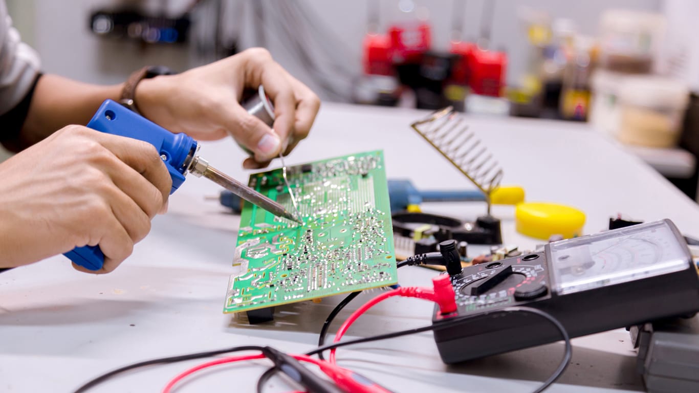
In the current digitally driven world, printed circuit boards (PCBs) are the unsung heroes behind all our devices. It could be your smartphone in the pocket or your laptop on the table, PCBs are a base for communication and functionality. However, what are those circuits made from? What plays the role of solder masks, Gerber files, and other factors to bring us the technology we use daily? Come with us to learn the intricacies of PCB assembly in simple language.
Introduction: Navigating the World of PCB Assembly
Picture this: as you’re holding the smartphone in your hand and look at its beautiful appearance, you’re amazed at how powerful it is. However, at its base lies a complex network of small components, all neatly arranged on a printed circuit board. This is where the magic is created – where solder mask, Gerber files, and solder flux come together and make your product a reality. In this guide, we will delve deep into the crux of PCB assembly, demystifying complex issues into simplified information. From the solder mask as a shield to the definition of Gerber files as roadmaps for manufacturing, we shall get acquainted with the key attributes of present-day electronics design. Imagine yourself being in the realm of modern technology, seeing yourself holding a polished smartphone whose shiny cover is telling stories about creation and power. However, there is a deeper layer beneath this, that is, a labyrinth of microscopic components ingeniously assembled onto a printed circuit board (PCB). It’s here, in this micro world, where the magic happens; where solder mask, Gerber files, and solder flux join in the music of creation to breathe life into your instrument. Get ready to embark on an incredible voyage through the center of PCB assembly, where complexity cooperates with clarity and invention rocks every step. Here, this in-depth guide will take you on a journey where we will unravel the secrets behind solder masks, Gerber files, and solder flux and help you understand them in the most simplified manner. Whether it’s the comfort like an angel guarding a soldier whole the fragile circuitry that comes from the protective embrace of the solder mask or the choreography of Gerber files that are the blueprint of manufacturing genius, we will unveil the threads that weave the fabric of modern electronics. Let’s dive into the intricate realm of PCB assembly, where each solder joint is imprinted with a history, and every digital schematic instills new inventions. We shall work hand in hand, and through this collaboration we will unravel the mysteries wrapped around our technological fabric, discovering the enigma and guile that serve as the pillars of our digital era. Are you ready to awaken, expand, and develop as we proceed through the beautiful world of contemporary electronics production?
Solder Mask: The Guardian of Precision
The respect for the core of each printed circuit board is an epoxy-based coating that resembles a barrier, which shields its elements from environmental factors. However, its goal is not only to ensure reliability – the solder mask also serves as a literal demarcation line for the solder to flow into during production. This provides the optimum connectivity and prohibits any bridging between the conducting paths. Visualize the same way that the solder mask is like the paint on a canvas, which both protects and visually distinguishes the underlying circuitry. The solder mask color going from bright colors to sleek monochromatic schemes is not only decorative, but it also helps with easy visual inspection, which is essential at the manufacturing stage, especially during quality control.
Gerber Files: Blueprinting Precision
Every PCB that you have seen in your neighborhood or your favorite storefront was crafted at some point on a computer, through a digital template known as Gerber files. These complex drawings represent the microscopic level of the board, focusing on the position of all the parts and the layout of the tracers so that they become the manufacturer’s reference in the process. Absent of the Gerber files, assembling a PCB will by now be as good as navigating a labyrinth while blindfolded – a wild and uncertain ride that will never allow you to succeed. With the evolvement of CAD software and digital fabrication technology, Gerber file creator program code Osamu’s easier, in the sense that, designers can create their visions with much more precision is what we have now than we used to have in the past. The board size bounds, stack-up layers’ arrangements, and component footprints are all present in these digital files that ensure production at the assembling level is accurate.
Solder Flux: The Silent Enabler
Attention-distributing tactic Taken as a granted factor, the crucial and yet the lesser-known part of the perfect solder joint is the solder flux. At times, it may be overlooked yet indispensable, PCB flux serves as an essential key component for the board assembly process to ensure a clean and irrefutable bonding of connections. It lets the metal remove the relevant surface oxidation, depress the liquid surface tension, and therefore solder melting to act more efficiently, as it does not play the role of an obstacle. Besides promoting metallurgy, fluxing offers benefits like preventing damaged wiring such as solder bridges and tombstoning, thus an increase in the production yield rate as well as products’ reliability. A multitude of solder flux formulations are created to meet many kinds of soldering, and the use of the right one is generally the key to having marvelous soldering results.
The Art of PCB Assembly: Harmonizing Precision and Ingenuity
PCB assembly is a complex partnership in which every participant plays a valuable part, from the rather ordinary solder mask to the precision Gerber files and also the quiet accomplice, solder flux. It’s an absolute orchestra of perfection and out-of-this-world intelligence, where every detail is intertwined to form a technological powerhouse. Heading deeper into the electronic world, let’s not fail to remember the hidden warriors that bring in new ideas. PCB masks, Gerber files, size, and solder flux, are the foundational bricks through which the future is created. Hence, that is when you hold a PCB in your hands, just marvel at the intricacies hidden within the surface of the PCB, and remember the journey throughout which it overcame various obstacles and made it to the surface.
Conclusion: Embracing the Future of PCB Assembly
Finally, we round off our journey into PCB assembly with a revelation of the delicate technique of masking and Gerber files along with tin solder flux. Unsung heroes remain unnoticed, hiding deep inside the electronics classes, but they are so important, interweaving precision, perfection, and innovation in one single thread to turn our techie vision into reality. With the protection of solder masks and the work of Gerber files not far behind involved in the creation of today’s electronics, each element works together as one to define this landscape. The more we admire our gadgets’ elegant appearance, the more we should not neglect the behind-the-scenes of the art and blueprint that took innumerable hours to create. Tackling the future of printed circuit board assembly together, we should continue creating unexpected results from our thirst for newness and our strong passion for innovation. Collectively, we should honor the unseen heroes of technology and a marvelous journey that displays our devices for us. By using solder masks, Gerber files, and solder flux, we can hurriedly move into tomorrow’s digital world where anything is possible.
FAQs
1. What is the main purpose of the solder mask in PCB assembly, and how does it affect the overall dependability of electronic devices?
While the solder mask has a protective role to play on printed circuit boards, guarding against the effects of the environment on the components and also acting as a separating line for soldiers during production. Its main task is to provide faultless operation by prohibiting short-circuiting and ensuring a proper connection between devices.
2. What is the essence of the use of Gerber files in the PCB manufacturing process, and what function may this serve?
Answer: The Gerber files which are in digital format are used for printing the Circuit Boards. They represent schematic diagrams on which components’ placement and wiring traces are indicated supplying the necessary reference for manufacturers to produce the printed circuit boards. Without Gerber files, PCB assembly would become a lucky game choosing one direction, instead of PCB fabrication using clear instructions.
3. Why is solder flux called a “silent enabler” when it plays an immensely significant part in the process of PCB assembly, even though it hardly even features in literature critics’ writings?
Solder flux, which is a vital but usually underestimated ingredient in printed circuit board (PCB) assembly, plays a significant role in the manufacturing process. It allows the construction of clean and refined solder joints via the elimination of surface oxidation, lowering liquid surface tension, and providing for efficient solder dissolving. Solder flux, although underrated, deserves respect for being a “silent enabler” that performs reliably in the background so the favored results are selling perfection.
4. What are the attractive features, in PCB manufacturing, that are associated with the application of different solder mask colors?
Various solder mask colors are utilized for both clean-up and aesthetic purposes in the PCB design. Beyond aesthetics, the colors enhance the ease of visual inspection during the manufacturing and quality control processes. The use of strikingly colored or plain geometric patterns that make the circuitry easy to spot by technicians is advantageous because it helps in the assembling process and leads to ensuring product quality.